the all laser approach sounds neat , a phonic cell that can store and return data… if the “dwell time” could be around the dwell of ram…
The dwell time of RAM and laser could assist in other applications too. It is just so like so neat. Really.
Attachments
That looks fun! 
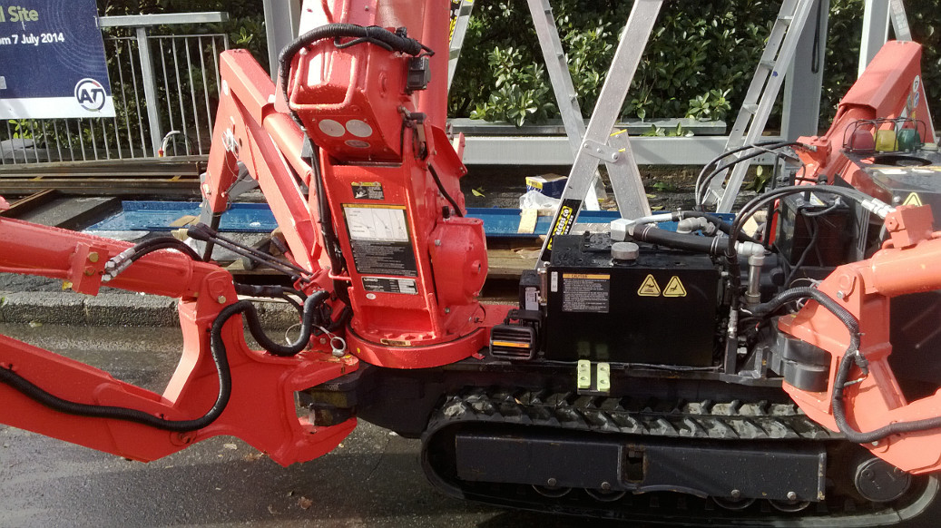
QuadTracktorsorus Welds?
Apparently it’s a machine that if I remember correctly serves as a mini crane. Fabulous little device. But as I try not to hijack topics, back to topic…something topic like related. Oh yeah…chips! In computers. They are sure progressing. With light in the current time too, to make something optical.
Attachments

http://www.research.ibm.com/cognitive-computing/neurosynaptic-chips.shtml#fbid=DHDi0HPIhVW
What is a cognitive chip? The latest SyNAPSE chip, introduced on August 7, 2014, has the potential to transform mobility by spurring innovation around an entirely new class of applications with sensory capabilities at incredibly low power levels. This is enabled by an revolutionary new technology design inspired by the human brain. IBM built a new chip with a brain-inspired computer architecture powered by an unprecedented 1 million neurons and 256 million synapses. It is the largest chip IBM has ever built at 5.4 billion transistors, and has an on-chip network of 4,096 neurosynaptic cores. Yet, it only consumes 70mW during real-time operation — orders of magnitude less energy than traditional chips. As part of a complete cognitive hardware and software ecosystem, this technology opens new computing frontiers for distributed sensor and supercomputing applications.
“We have made optical systems at the microscopic scale that amplify light and produce ultra-narrowband spectral output,” explained J. Gary Eden, a professor of electrical and computer engineering (ECE) at Illinois. "These new optical amplifiers are well-suited for routing optical power on a chip containing both electronic and optical components.
Most of today’s electronic products consist of traditional made parts. Plastic molded housings containing PCB’s with soldered THT and SMT components. In many cases even the design of a product is based on the electronics that should fit inside! Shouldn’t it be the other way around? Shouldn’t the electronics be a part of the design based on ergonomics and aesthetics?
How about static memory a la quantum coherence? When photons are absorbed by atoms the electron/s move to higher shelves or energy states. That energy state tends to degrade and a photon is given off. This is uncontrollably probabilistic.
I don’t think your actually talking about a photonic computer. I think your talking about fiber optic PCBs, which is pretty damned cool just the same.
On the other hand; if you have solved the quantum coherence problem then please contact Geordie Rose. He’ll make you friggin’ rich.
No, what I am thinking,
Recieve power - EMF (brodcast power-
Send data laser rgb via 12 outputs
Like up left,
Up left back,
Back,
Forward,
This way a networkof stackable cubes, on top of a mat, could be a computer,
Think fiber optic lego pc, and each part can be a differing piece, but all are networking nodes,
So, HP photonic interconnects, built in 3d, and laser emmiters, and a device, in each cube.
Princeton researchers demonstrated a novel type of microwave laser – called a maser – so small that’s the size of a grain of rice. The laser is powered by individual electrons that tunnel through artificial atoms known as quantum dots.
This +
http://www.toshiba-europe.com/research/crl/QIG/pdfs/singlephotondetection/spd_jjap_Jan01.PDF
= my computer.
ok the deal is sealed, now a optical computer can be distributed across a room,
remember my 3d logic node system?
it just got real…
now I see
a power beam,
reciever beam
brodcast beam
this way, a hub, can power, feed data and recieve error data using a mems array to feed an array of chips, and then recieve feedback data.
if a chip is powered without wires, sends data without wire, and recieves data without wires, a true 100% scalable architecture can be achieved.
It’s an interesting take on the problem of trying to keep the upward trend in performance, but what does this have to do with optics?
This could’ve been posted as a new thread rather than digging down 4 years to bump this one.
I said that the future of computing is small nodes with self contained ram/proccessor
I think one could have ‘states’ and complex logic in these self contained cells,
so that depending on the problems being solved the architecture can change.
this is a step in that direction, however it’s not a grid sending / receiving light yet
(think of GLSL nodes that instead are real hardware and switch states to perform specific operations very fast and data flows both ways on the node graph.)
this is cool,
one may be able to manipulate a laser en-route without absorbing it ![]()
If its R B G , then its not like current computer, a binary system / off & one state , but a tertiary system. Just a thought

binary 2 ** 8 = 256 mb ram
tertiary 3 ** 9 = 19 683 mb ram